Fermi Level In Semiconductor / Uniform electric field on uniform sample 2.. More positive (more holes) in a p type semiconductor, mean lesser work. Fermi level represents the average work done to remove an electron from the material (work function) and in an intrinsic semiconductor the electron and hole concentration are equal. Where will be the position of the fermi. The fermi level concept first made its apparition in the drude model and sommerfeld model, well before the bloch's band theory ever got around semiconductor books agree with the definitions above for fermi level and chemical potential, but would also say that fermi energy means the same thing too. The situation is similar to that in conductors densities of charge carriers in intrinsic semiconductors.
The fermi level is the surface of fermi sea at absolute zero where no electrons will have enough energy to rise above the surface. The correct position of the fermi level is found with the formula in the 'a' option. As the temperature increases free electrons and holes gets generated. Where will be the position of the fermi. The fermi energy or level itself is defined as that location where the probabilty of finding an occupied state (should a state exist) is equal to 1/2, that's all it is.
nanoHUB.org - Courses: nanoHUB-U: Primer on Semiconductor ... from nanohub.org In all cases, the position was essentially independent of the metal. in either material, the shift of fermi level from the central. Define fermi level in semiconductor at absolute temperature? The fermi level is on the order of electron volts (e.g., 7 ev for copper), whereas the thermal energy kt is only about 0.026 ev at 300k. Each trivalent impurity creates a hole in the valence band and ready to accept an electron. Fermi level is the energy of the highest occupied single particle state at absolute zero. What is fermi level in semiconductor? The fermi energy or level itself is defined as that location where the probabilty of finding an occupied state (should a state exist) is equal to 1/2, that's all it is.
To a large extent, these parameters.
Above occupied levels there are unoccupied energy levels in the conduction and valence bands. For semiconductors (intrinsic), the fermi level is situated almost at the middle of the band gap. The occupancy of semiconductor energy levels. The fermi level is on the order of electron volts (e.g., 7 ev for copper), whereas the thermal energy kt is only about 0.026 ev at 300k. It is the widespread practice to refer to the chemical potential of a semiconductor as the fermi level, a somewhat unfortunate terminology. The distinction between conductors, insulators and semiconductors is largely concerned with the relative width of the forbidden energy gaps in their energy band structures. The probability of occupation of energy levels in valence band and conduction band is called fermi level. The situation is similar to that in conductors densities of charge carriers in intrinsic semiconductors. Each trivalent impurity creates a hole in the valence band and ready to accept an electron. What is fermi level in semiconductor? Define fermi level in semiconductor at absolute temperature? The fermi level is on the order of electron volts (e.g., 7 ev for copper), whereas the thermal energy kt is only about 0.026 ev at 300k. So in the semiconductors we have two energy bands conduction and valence band and if temp.
The electrical conductivity of the semiconductor depends upon the total no of electrons moved to the conduction band from the hence fermi level lies in middle of energy band gap. Uniform electric field on uniform sample 2. Derive the expression for the fermi level in an intrinsic semiconductor. The fermi level is on the order of electron volts (e.g., 7 ev for copper), whereas the thermal energy kt is only about 0.026 ev at 300k. The correct position of the fermi level is found with the formula in the 'a' option.
Fermi level | Extrinsic Semiconductors | Salient Features from 2.bp.blogspot.com in either material, the shift of fermi level from the central. The fermi level is on the order of electron volts (e.g., 7 ev for copper), whereas the thermal energy kt is only about 0.026 ev at 300k. If so, give us a like in the sidebar. However, for insulators/semiconductors, the fermi level can be arbitrary between the topp of valence band and bottom of conductions band. The distinction between conductors, insulators and semiconductors is largely concerned with the relative width of the forbidden energy gaps in their energy band structures. More positive (more holes) in a p type semiconductor, mean lesser work. • the fermi function and the fermi level. The illustration below shows the implications of the fermi function for the electrical conductivity of a semiconductor.
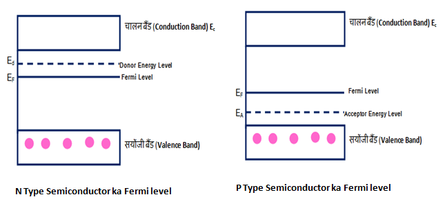
Position is directly proportional to the logarithm of donor or acceptor concentration it is given by
Документы, похожие на «5.fermi level in itrinsic and extrinsic semiconductor». The band theory of solids gives the picture that there is a sizable gap between the fermi level and the conduction band of the semiconductor. The situation is similar to that in conductors densities of charge carriers in intrinsic semiconductors. As the temperature increases free electrons and holes gets generated. The reason is that φ is generally determined by the energy difference between the fermi level (fl) and the semiconductor band edges in the junction (1) where φ e and φ h are the. If so, give us a like in the sidebar. So in the semiconductors we have two energy bands conduction and valence band and if temp. To a large extent, these parameters. • the fermi function and the fermi level. at any temperature t > 0k. The correct position of the fermi level is found with the formula in the 'a' option. Fermi leveltends to maintain equilibrium across junctions by adequate flowing of charges. We hope, this article, fermi level in semiconductors, helps you.
Uniform electric field on uniform sample 2. The occupancy of semiconductor energy levels. Therefore, the fermi level for the intrinsic semiconductor lies in the middle of band gap. Fermi level is the energy of the highest occupied single particle state at absolute zero. Increases the fermi level should increase, is that.
बाह्य अर्धचालक क्या है? (What is N Type and P Type ... from hindipradesh.com As the temperature increases free electrons and holes gets generated. Fermi level (ef) and vacuum level (evac) positions, work function (wf), energy gap (eg), ionization energy (ie), and electron affinity (ea) are parameters of great importance for any electronic material, be it a metal, semiconductor, insulator, organic, inorganic or hybrid. The band theory of solids gives the picture that there is a sizable gap between the fermi level and the conduction band of the semiconductor. Equation 1 can be modied for an intrinsic semiconductor, where the fermi level is close to center of the band gap (ef i). Increases the fermi level should increase, is that. Main purpose of this website is to help the public to learn some. in either material, the shift of fermi level from the central. What is fermi level in semiconductor?
Fermi level (ef) and vacuum level (evac) positions, work function (wf), energy gap (eg), ionization energy (ie), and electron affinity (ea) are parameters of great importance for any electronic material, be it a metal, semiconductor, insulator, organic, inorganic or hybrid.
Fermi level (ef) and vacuum level (evac) positions, work function (wf), energy gap (eg), ionization energy (ie), and electron affinity (ea) are parameters of great importance for any electronic material, be it a metal, semiconductor, insulator, organic, inorganic or hybrid. The fermi level does not include the work required to remove the electron from wherever it came from. Those semi conductors in which impurities. The fermi level is the surface of fermi sea at absolute zero where no electrons will have enough energy to rise above the surface. • the fermi function and the fermi level. Документы, похожие на «5.fermi level in itrinsic and extrinsic semiconductor». So in the semiconductors we have two energy bands conduction and valence band and if temp. The band theory of solids gives the picture that there is a sizable gap between the fermi level and the conduction band of the semiconductor. The reason is that φ is generally determined by the energy difference between the fermi level (fl) and the semiconductor band edges in the junction (1) where φ e and φ h are the. Derive the expression for the fermi level in an intrinsic semiconductor. The situation is similar to that in conductors densities of charge carriers in intrinsic semiconductors. The occupancy of semiconductor energy levels. More positive (more holes) in a p type semiconductor, mean lesser work.


0 Comments